Samsung n770f lite schematics note10 Note4 galaxy note 4 smart phone repair reference schematic pcb board Schematics n900
Patrice Benoit Art: [45+] Note 4 Schematic Diagram
Samsung galaxy note10+ schematics Jalur solusion n910 sekitaran luar perhatikan perlu bagian cek dioda Oppo schematics
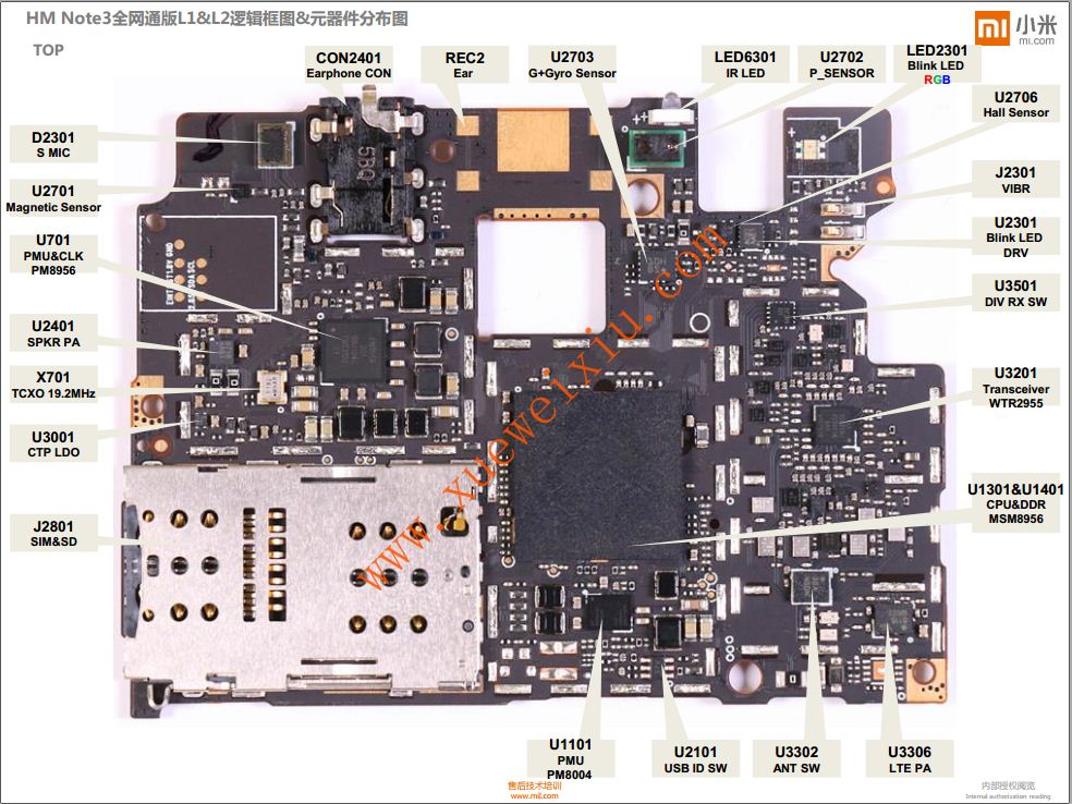
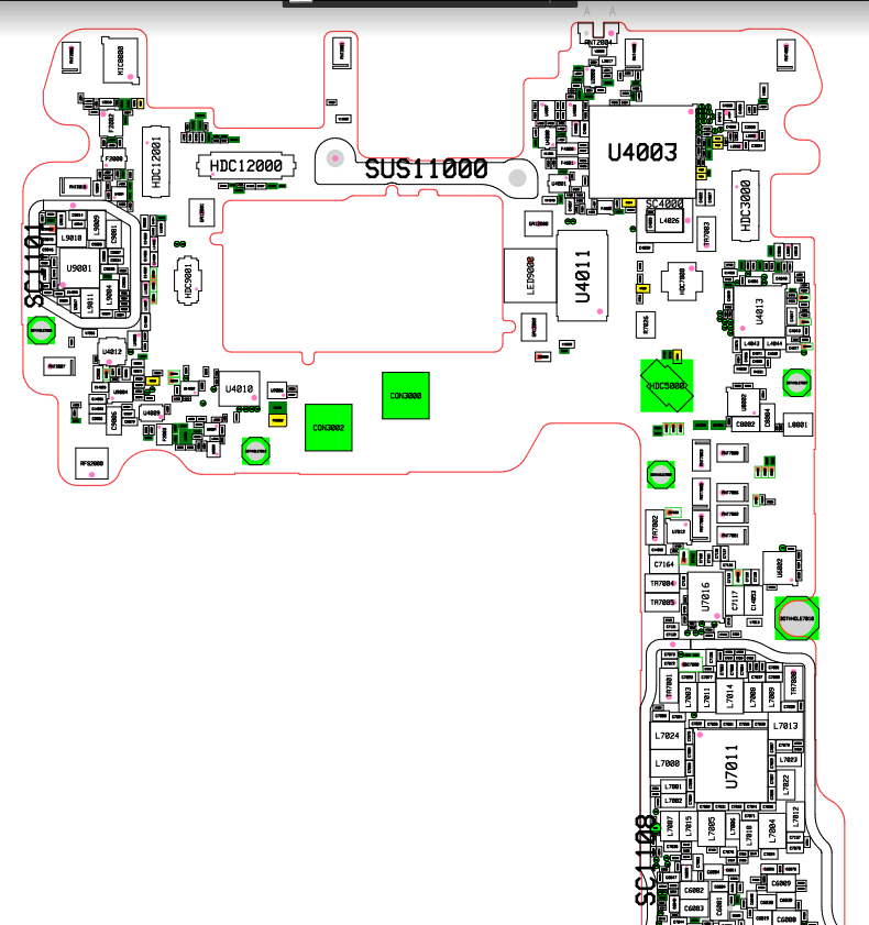
Redmi note 3 pro (qualcomm) schematic & layout diagrams
Samsung galaxy note 3 sm-n900 lcd dispaly not working solutionN900 lcd samsung galaxy sm note solution working not Patrice benoit art: [45+] note 4 schematic diagramSamsung galaxy note10 lite / sm-n770f schematics.
Pro redmi note schematic xiaomi qualcomm jmh diagramsSchematics samsung note 9 sm-n960n Samsung galaxy note10 sm-n970f schematicsDiagram note schematic galaxy pcb manual board note4 maintenance reference repair smart phone electronic.

Schematic samsung galaxy note 4 charger data hardware solusion (sm-n910
Samsung note 8 sm-n950u pcb layout &teardownSchematics note10 sm n975u Note samsung galaxy diagram circuit ic n9005 n900 disassembly numberSamsung galaxy note 3 circuit diagram : r/mobilerepair.
Galaxy disassembly myfixguideSamsung galaxy note 3 sm-n900 schematics Patrice benoit art: [45+] note 4 schematic diagramSchematics note10 n970f sm.
Teardown techinsights n910c note4
.
.


Samsung Galaxy Note10 Lite / SM-N770F schematics
Schematics Samsung Note 9 SM-N960N - Mobile Software
Samsung Galaxy Note 3 Circuit Diagram : r/mobilerepair

Samsung Galaxy Note10 SM-N970F schematics

Samsung Galaxy Note 3 SM-N900 LCD Dispaly not Working Solution
Samsung galaxy note 3 SM-N900 schematics
![Patrice Benoit Art: [45+] Note 4 Schematic Diagram](https://i2.wp.com/www.techinsights.com/sites/default/files/2019-04/note4-note-alpha-Galaxy-Note-4-Board-Shots-1.jpg)
Patrice Benoit Art: [45+] Note 4 Schematic Diagram

NOTE4 GALAXY Note 4 smart phone repair reference Schematic PCB board
Samsung Note 8 SM-N950U Pcb Layout &Teardown